8 Bit Shift Register Truth Table
The M74HC165 is an high speed CMOS 8 BIT PISO SHIFT REGISTER fabricated with silicon gate C2MOS technology. Output Voltage is equal to Operating voltage.
Shift Registers In Digital Logic Geeksforgeeks
The internal logic diagram of 74LS232 shift register IC is shown in the figure below.
. Figure 1 shows a n-bit synchronous SISO shift register sensitive to positive edge of the clock pulse. Here the data word which is to be stored is fed bit-by-bit at the input of the first flip-flop. Following are the four types of shift registers based on applying inputs and accessing of outputs.
Serial In Serial Out SISO shift registers are a kind of shift registers where both data loading as well as data retrieval tofrom the shift register occurs in serial-mode. The logic diagram and logic block are shown in Figure 31 ab. IC 40104 4 bit bidirectional Parallel-inParallel-out PIPO Shift Register.
These flip-flops make transitions of data on the positive edge of the clock only. With an additional shift-register we could have easily controlled 14 outputs off the same 3 pins. 8-Bit Parallel-Out Serial Shift Registers datasheet.
In Proteus 8 Build an 8 bit shift register with load and shift-left shift-right with its truth table. In Proteus 8 Build an 8 bit shift register with load and shift-left shift-right with its truth table. IC 40195 4-bit universal shift register.
PD CPD x VCC 2 x f i CL x VCC 2 x f o where. Module shiftclk si so. 7 rows 74LS166 is an 8-bit shift register digital IC.
Shift Register is a group of flip flops used to store multiple bits of data. IC 4021 8-bit static shift register. 9 rows The 74HC164 is a 8-bit edge-triggered shift registers with serial data entry and an output.
Free easy returns on millions of items. Fi input frequency in MHz. Truth Table for working of 74LS323 is shown in the figure below.
A good example of a parallel in serial out shift register is the 74HC165 8-bit shift register although it can also be operated as a serial in serial out shift register. In Proteus 8 Build an. Figure 346b Timing diagram of a 74HC164 8-bit Serial InParallel Out Shift Register In the timing diagram the register is cleared asynchronously by activating the active- low CLR input at interval t.
A serial-in serial-out shift register may be one to 64 bits in length longer if registers or packages are cascaded. Circuit with 1 Shift Register. An n-bit shift register can be formed by connecting n flip-flops where each flip flop stores a single bit of data.
Considering the above table let us have a look at the waveform representation of a SISO shift register. 74HCT595 are high-speed Si-g ate CMOS devices and are pin compatible with Low-power Schottky TTL LSTTL. In cased of 8-bit parallel communication.
The SN74LS166 8-bit shift register comes with 9 data ip pins of which 8 of them are parallel input pins and the final one is a serial input pin. The below code is for a Shift Left Register of 8 bits Serial In and Serial Out with a Positive edge. IC 7491 8-bit shift register serial-in serial-out gated input.
The 74LVC594A is an 8-bit serial-inserial or parallel-out shift register with a storage register. Insert the new element at one end of the vector while simultaneously shifting all of the others one place closer to the output side. IC 7495 4-bit shift register parallel in parallel-out serial input.
The logical circuit diagram of the SN74LS166 8-bit shift register is shown in the figure below. The bits stored in registers shifted when the clock pulse is applied within and inside or outside the registers. Serial-in serial-out shift registers delay data by one clock time for each stage.
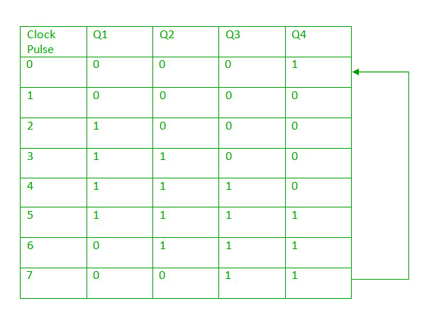
The device features a serial data input DS eight parallel data inputs D0 to D7 and two complementary serial outputs Q7 and Q7. Clear FF0 FF1 FF2 FF3 1001 0 0 0 0 1 0 0 0 0 1 0 0 0 0 1 0 1 0 0 1. If the register is capable of shifting bits either towards right hand side or towards left hand side is known as shift register.
This device contains eight clocked master slave RS flip-flops connected as a shift register with auxiliary gating to provide over-riding asynchronous parallel entry. The device features a serial input DS and a serial output Q7S to enable cascading. 1 8-bit shift-left register with positive-edge clock serial In and serial out.
An N bit shift register contains N flip-flops. Put the code in a clocked process and tap the last bit in the vector and you have your shift register. 135V Vcc45V Can be easily cascaded with more IC to get more outputs.
315V Vcc45V Maximum low-level Input Voltage. IC 4015 Dual 4-stage shift register. They are specified in compliance with JEDEC standard No.
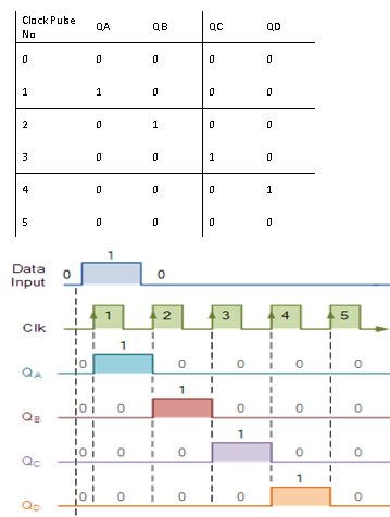
Here the first figure shows the clock input signal while the second figure shows the data input to be stored which is 1111 for this particular case. The bits stored in such registers can be made to move within the registers and inout of the registers by applying clock pulses. A group of flip flops which is used to store multiple bits of data and the data is moved from one flip flop to another is known as Shift Register.
8-bit universal shift register. To form an n-bit shift register we have to connect n number of flip. Separate clock and reset inputs are provided on both shift and storage registers.
Parallel data enters when the shiftload input is low. 3-state 25 C -40 C to 85 C-40 C to 125 C Symbol Parameter Conditions Min Typ Max Min Max Min Max Unit CPD power dissipation capacitance VI GND to VCC 1 - 120 - - - - - pF 1 CPD is used to determine the dynamic power dissipation PD in μW. The above are some of the applications of shift registers.
74HCT595 8-bit serial-in serial or parallel-out shift register with output latches. See the answer See the answer See the answer done loading. Minimum high-level Input Voltage.
Ad Free shipping on qualified orders. 8-bit Serial In Parallel out Shift register. Browse discover thousands of brands.
By using the register we were able to control 7 outputs with only 3 stamps pins. Verilog Code For Shift Register. They will store a bit of data for each register.
The most straightforward way to create a shift register is to use vector slicing. Circuit Diagram of SN74LS166 8-Bit Shift Register. It consists of a number of AND OR NAND NOT gates and 8 edge-triggered D type Flip-Flops.
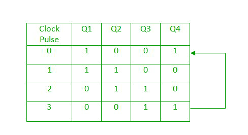
The figure below represents the truth table for the 4-bit SISO shift register. Since we were limited by the number of pins on a basic stamp we used the 8-bit Shift register to demux a signal to multiple outputs. Read customer reviews find best sellers.
Always posedge clk begin. 31 An 8-bit serial inparallel out shift register 74HC164 The 74HC164 is an example of an IC shift register having serial inparallel out operation. Data is shifted on the LOW-to-HIGH transitions of the SHCP input and the data in the shift register is transferred to.
This problem has been solved.

Shift Register Parallel And Serial Shift Register
Shift Registers In Digital Logic Geeksforgeeks
Sequential Logic Circuits Electronics Tutorial


Comments
Post a Comment